
Nov 22: Article "Non-destructive Characterization of Films via White Light Reflectance Spectroscopy"
|
In this work, we consider White Light Reflectance Spectroscopy (WLRS) as an optical methodology for the accurate, fast and non-destructive measurement of film thickness in the 1 nm to the 1 mm range and for applications that include microelectronics, photonics, bioanalysis and packaging. Films to which WLRS is applicable can be either homogeneous or layered-composite ones, while thickness and composition might be fixed or arying with time; in the latter case, real-time monitoring of the kinetics of processes such as certain transitions, film dissolution and bioreactions is possible. We present the basic principles of WLRS and a selection of characteristic application examples of current interest, and we also briefly compare WLRS with alternative methods for film measurement. |
| D. Goustouridis, I. Raptis, Th. Mpatzaka, S. Fournari, G. Zisis, P. Petrou, K. Beltsios Micro 2, 495(2022) “Non-destructive Characterization of Selected Types of Films and Other Layers via White Light Reflectance Spectroscopy (WLRS)” |
|
Spectroscopic reflectance is a versatile optical methodology for the characterization of transparent and semi-transparent thin films in terms of thickness and refractive index. The Fresnel equations are used to interpret the measurements, but their accuracy is limited when surface roughness is present. Nanoroughness can be modelled through a discretized multi-slice and effective medium approach, but to date, this offered mostly qualitative and not quantitative accuracy. Here we introduce an adaptive and nonlocal effective medium approach, which considers the relative size and environment of each discretized slice. We develop our model using finite-difference time-domain simulation results and demonstrate its ability to predict nanoroughness size and shape with relative errors < 3% in a variety of test systems. The accuracy of the model is directly compared to the prediction capabilities of the Bruggeman and Maxwell–Garnett models, highlighting its superiority. Our model is fully parametrized and ready to use for exploring the effects of roughness on reflectance without the need for costly 3D simulations and to be integrated into the Fresnel simulator of spectroscopic reflectance tools. |
| El.Lampadariou, K.Kaklamanis, D.Goustouridis, I.Raptis, El.Lidorikis Photonics 9 499(2022) “Nonlocal effective medium (NLEM) for quantitative modelling of nanoroughness in spectroscopic reflectance”” |
|
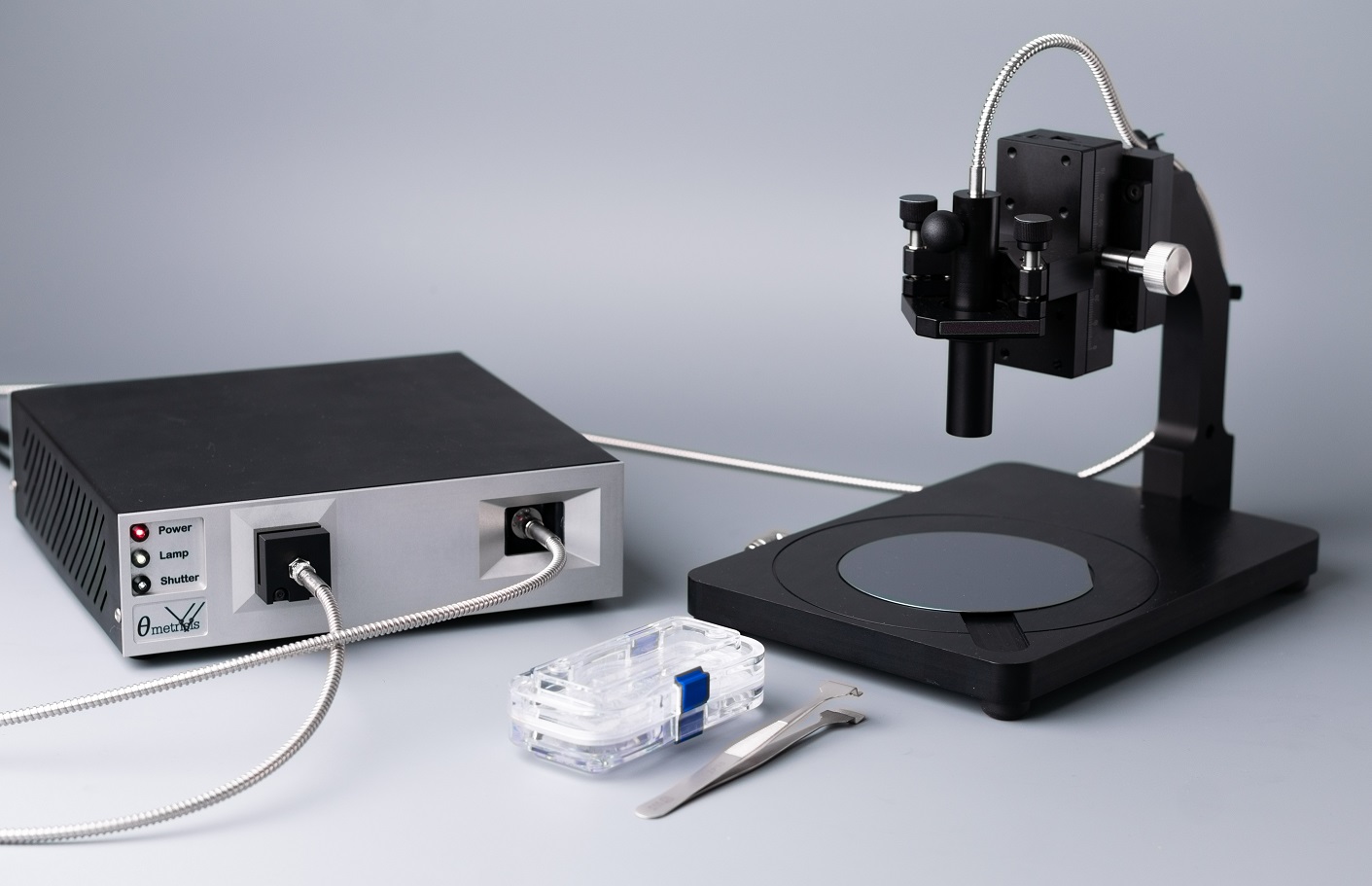
A new product, FR-ES is released. FR-ES is a compact entry level tool that is designed to provide an excellent performance in terms of characterization of coatings. It can be employed in a wide range of diverse applications, such as: Film thickness, Refractive Index, Color, Transmittance, Reflectance, and many more. There are three configurations available:
The tool can be accompanied by a wide range of Accessories, such as: Filters to block light at certain spectral regimes, FR-Mic for measurements at very small areas, Manual stage, 25x25mm, 100x100mm or 200x200mm Film/Cuvette Holder for Absorbance / Transmittance and chemical concentration measurements, Integration Spheres for diffuse & total reflectance |
 |
For more information please contact our sales team at: This email address is being protected from spambots. You need JavaScript enabled to view it.
Dec 20: Article "In-situ characterization of the development step of high-resolution e-beam resists"
|
The optimization of the development conditions in a lithography process is crucial for the overall lithographic performance while the study of the development step provides useful information regarding the properties of the lithographic material. In this work, high resolution e-beam resists are studied through in-situ monitoring of resist thickness evolution during the development step. In-situ monitoring of the resist thickness is conducted through fitting of the spectroscopic reflectance of resist films coated on dielectric layers on Si wafers and by using light at wavelengths that do not modify the lithographic properties of the resist film. The methodology was applied in the case of two selected commercially available high resolution e-beam resists and the dissolution process was monitored in depth. The recorded results prove that in-situ dissolution monitoring is a powerful tool for the generation of experimentally based development models for the lithographic materials employed in high resolution lithography. These dissolution rate (DR) values could be correlated with energy deposition profiles due to e-beam exposure and used as input in e-beam lithography (EBL) simulation tools in order to improve the accuracy of the simulation and decrease the number of actual test exposures for process optimization. |
| Th.Mpatzaka, G.Papageorgiou, N.Papanikolaou, E.Valamontes, Th.Ganetsos, D.Goustouridis, I.Raptis, G.Zisis Microelectron. Eng. 9 100070(2020) “In-situ characterization of the development step of high-resolution e-beam resists”” |
|
In the past 2 decades silsesquioxane has gained attention in the Electron Beam Lithography community as a negative tone electron-sensitive resist (HSQ) whose advantages (sub-20 nm resolution, high contrast, low Line Edge Roughness, good shape fidelity and high etch resistance) outnumber its associated drawbacks (limited shelf-life, chemical instability issues, process residuals, low sensitivity, cost). The new silsesquioxane based resist, developed by Allresist GmbH, Medusa 82 (official product name: SX AR-N 8200) and Medusa 82 UV (SX AR-N 8250), its highly sensitive counterpart, have been designed to address all these issues. The objective of this work is to use fundamental Contrast Curve analysis, Dissolution Monitoring and parametric e-beam lithography experiments to study the influence of processing conditions (Post Exposure Bake Temperature, Development duration and developer strength) on the lithographic performance of sub-40 nm thick films. |
| Th.Mpatzaka, G.Zisis, I.Raptis, V.Vamvakas, Ch.Kaiser, T.Mai, M.Schirmer, M.Gerngroß, G.Papageorgiou, Micro Nano Eng. 8 100065(2020) “Process study and the lithographic performance of commercially available silsesquioxane based electron sensitive resist Medusa 82” |
|
Axl Imperial Ltd. and ThetaMetrisis have signed an agreement for the distribution of ThetaMetrisis products in the industrial markets of Greece and Cyprus. Prospective customers from this area are kindly requested to contact the Axl Imperal Ltd sales team for further information on ThetaMetrisis products and demonstration of their capabilities. Mr. George RakanidesTel: +30 210 725 7712 Website: https://axlimperial.com/ |
|
I & A Technology Inc. and ThetaMetrisis have signed an agreement for the distribution of ThetaMetrisis products in the market of South Korea. Prospective customers from this area are kindly requested to contact the I & A Technology sales team for further information on ThetaMetrisis products and demonstration of their capabilities. Tel: +82-31-203-7978 Website: http://ina-technology.com/ |
|
Biosensing through White Light Reflectance Spectroscopy (WLRS) is based on monitoring the shift of interference spectrum due to the binding reactions occurring on top of a thin SiO2 layer deposited on a silicon chip. Multianalyte determinations were possible through scanning of a single sensor chip on which multiple bioreactive areas have been created. Nonetheless, the implementation of moving parts increased the instrumentation size and complexity and limited the potential for on-site determinations. Thus, in this work, a new approach, which is based on patterning the sensor surface to create areas with different SiO2 thickness, is developed and evaluated for multi-analyte determinations with the WLRS set-up. The areas of different thickness can be interrogated by a single reflection probe placed on a fixed position over the chip and the reflection spectrum recorded is deconvoluted to the spectra corresponding to each area allowing the simultaneous monitoring of the bioreactions taking place at each one of them. The combination of different areas thickness was optimized using chips with two areas for single analyte assays. The optimum chips were then used for the simultaneous determination of two mycotoxins, aflatoxin B1 and fumonisin B1. A competitive immunoassay format was followed employing immobilization of mycotoxin-protein conjugates onto the SiO2 of different thickness. It was found that the dual-analyte assays had identical analytical characteristics with the respective single-analyte ones. The detection limits achieved were 0.05 ng/mL for aflatoxin B1 and 1.0 ng/mL for fumonisin B1, with dynamic ranges extending up to 5.0 and 50 ng/mL, respectively. The sensor was also evaluated for the determination of the two mycotoxins in whole grain samples (wheat and maize). The extraction protocol was optimized and recoveries ranging from 85 to 115% have been determined. Due to lack of moving parts, the novel multi-analyte format is expected to considerably facilitate the built-up of a portable device for determination of analytes at the point-of-need. |
| V. Anastasiadis, G. Koukouvinos, P.S. Petrou, A. Economou, M. Harjanne, P. Heimala, D. Goustouridis, I. Raptis, S.E. Kakabakos Biosens. Bioelectron. 153 112035(2020) “Multiplexed mycotoxins determination employing white light reflectance spectroscopy and silicon chips with silicon oxide areas of different thickness” |
|
MICL Consulting & Logistics and ThetaMetrisis has signed an agreement for the distribution of ThetaMetrisis products in the market of Israel. Prospective customers from Israel are kindly requested to contact the MICL sales team for further information on ThetaMetrisis products and demonstration of their capabilities. Tel: +972-4-8343966 Email: This email address is being protected from spambots. You need JavaScript enabled to view it. Website: https://micl-group.com/ |