|
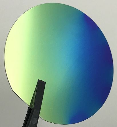
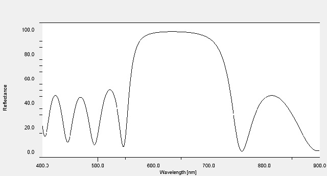
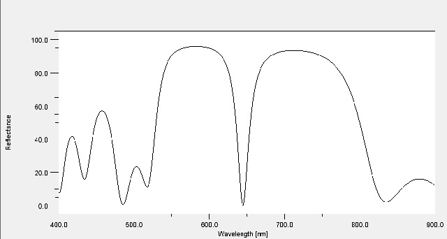
Thin and thick dielectric films are used in a wide range of industrial sectors such as semiconductors, photonics and optics. The detailed characterization of those films is of paramount importance for optimum device performance, higher yield and lower production cost. Among the various parameters that need to be measured film thickness and optical properties (colour, refractive index, reflectance, transmittance) are of high importance. For example, in semiconductor industry dielectric films such as SiO2, Si3N4, HfO2 are widely used. In several cases, stoichiometry of the film might differ from the desired one with negative impact on the device performance either from electrical or optical losses point of view. Thus it is important to measure both film thickness and refractive index of the film simultaneously. FR-tools can characterize dielectric films in a very broad thickness range: from 1nanometer (thermally grown SiO2/Si case) up to 1000microns or more (glass). In addition, FR-tools can measure the refractive index along with the film thickness for films >50nm. In cases where mapping of thickness an/or refractive index is required, e.g. dielectrics on wafers, FR-pRo tools are combined with robust and fast RΘ or XY stages for automatic characterization of the desired parameters. Furthermore, for patterned dielectric films, FR-pRo tools can be combines with FR-Mic and characterize dielectric patterns with ultra fine spot size, down to very few micrometers. |
|
Typical Application Notes:


