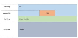
There several applications where more than one layers are applied on a substrate. E.g. in the realization od semiconductor devices, in planar photonics, in opthalmiatric lenses, in antireflective coatings etc.

FR-tools and FR-monitor software allow for the simultaneous and accurate measurement of the individual thicknesses of multiple layers. In particular, ThetaMetrisis solutions have been proved capable in the accurate determination of the thicknesses of multilayers within a wide range of diverse applications and with individual thicknesses from few nanometers such as:

  • Si3N4/SiO2/Si for semiconductor devices
  • Resist/Si3N4/SiO2/Si for semiconductor devices and planar waveguides
  • SiO2/Si3N4/SiO2/Si for planar waveguides
  • AntiFogging and HardCoat for automotive headlights
  • HardCoat and IntemediateLayer for protective sheets.

Furthermore, FR-Monitor provides the concept of linked layers that allow the characterization of antireflective layers in bilayer and trilayer stacks .

 photoresist


photoresist


 photoresist


Typical Application Notes:                                                          

App004- Reflectance of stack of films
App005- Stack of films
App026- Thickness measurement of Perovskites films
App035 - Local core and cladding thickness determination of planar waveguides
App036 - Suspended Active-Silicon membrane thickness measurements for MEMS applications
App038 - Fast and Accurate mapping of layers thicknesses of SOI wafers.

Go to top

ThetaMetrisis - Copyright (©) 2019 All Rights Reserved


Our website is protected by DMC Firewall!