
|
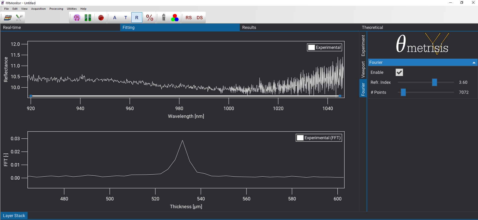
Silicon is the fundamental material for electronics industry. Its unique properties along with the huge investments in manpower and infrastructure, both in research and industry, revolutionize our world during the last decades. Nowadays, Si wafers with diameter of 300mm and even 450mm are routinely manufactured and processed for the realization of high-end ICs at low cost. In modern integrated circuits industry, the measurement of Si thickness is of high interest with particular emphasis in Si membranes, Si wafer and failure analysis. The high absorbance of Si in UV/VIS/NIR up to 1100nm wavelength make the thickness measurement of Si wafers a challenging task. Si membranes: In several MEMs devices, a free standing Si membrane is employed e.g. as flow sensing element , in pressure sensors. These membranes are manufactured by various techniques such as back-side lapping, on SOI wafer, by Si-wafer bonding etc. It is critical to measure accurately the Si thickness by a fast and non-contact method given the limited mechanical strength of those membranes and check if the membrane is within the specifications (thickness, uniformity). Si wafer: 300-mm diameter wafers are 775 μm thick to ensure safe wafer manufacturing without breakage and to provide sufficient mechanical and thermal stability of the wafers in IC fabrication during processing steps of lithography and heat treatments. Furthermore, Si wafers should meet certain defect kinetic properties in device processing, which depend on the wafer thickness as well and are crucial for device yield and economic feasibility. Failure Analysis: For the location and identification of defects that affect the operation of an IC, it is critical to back-thin the Si die/wafer at a very thin and uniform layer that allows for the inspection of the defective area by standard microscopes. ThetaMetrisis offers a wide range of compact and robust tools with unique advantages in performance and price that fulfill the needs for the measurement of Si thickness ranging from few nanometers and up to 1millimeter. E.g. FR-pRo NIR-N2 tool that operates in the 900-1050nm spectral range is capable for thickness measurement up to standard 4inch Si wafers. The same tool when accompanied with FR-Mic becomes the ideal tool for measurement thickness in failure analysis of rough Si dies with measurement of 200μm thick Si dies already demonstrated. |
  |
Typical Application Notes: