
|
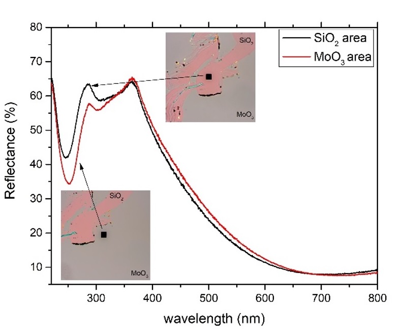
Two-dimensional (2D) materials, are crystalline materials consisting of a single layer of atoms. Graphene was the first ‘modern’ 2D material to be isolated in 2004. Since then, there have been hundreds of other examples, with an extensive range of properties. These materials have found use in applications such as photovoltaics, semiconductors, electrodes and water purification. Some 700 2D materials have been predicted to be stable, although many remain to be synthesized. The global market for 2D materials is expected to reach US$390 million by 2025, mostly for graphene in the semiconductor, electronics, battery energy and composite materials markets. FR-tools operating in the UV range are capable to measure ultra-thin layers, down to 1nm, e.g. SiO2 on Si. By employing the FR-pRo UV/VIS tool it is possible to measure even thinner layers when these layers are applied on certain substrates, e.g. SiO2/Si. In particular, FR-pRo UV/VIS has successfully measured the thickness of graphene and MoS2 layers on certain substrates and was able to distinguish between the areas without 2-D material and the areas with more than one 2-D layers. |
|
Typical Application Notes: