|
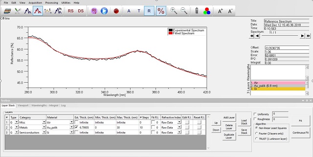
In electronics industry, metal films are usually of several micrometers or several tens of micrometers thick to successfully serve as conductors with low losses. Such kind of metallic films are totally opaque to the spectral range of reflectance/transmittance tools. However, in large area electronics, e.g. LCDs, OLEDs a thin optically transparent conducting layer is required with Transparent Conducting Oxides (TCOs) to be the first choice. However, TCOs typically exhibit some limitations e.g. exposure, difficulties to be applied on flexible substrates due to cracking. On the other hand, very thin metallic films can be employed in such applications since the transparency of metallic films drops exponentially with thickness, while the sheet resistance increases rapidly. In addition, thin metallic layers are also good candidates for photonic structures (e.g. cladding layers) and in biosensors (e.g. SPR). By using FR-tools, the thickness of thin and ultra-thin metallic layers can be accurately measured either in reflectance or transmittance mode. By employing spectral reflectance set-ups, the maximum metallic film thickness that can be measured is 40-50nm. On the other hand, by monitoring the absorbance at characteristic wavelengths, quite thicker metallic films deposited on transparent substrates can be characterized. Due to the differences between the absorbance characteristics between the various metals, the maximum thickness for silver is ~300nm, for gold is ~500nm and for aluminum is ~900nm. |
 |
Typical Application Notes:
