
|
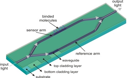
Photonic Integrated Circuits (PICs) are devices on which several or even many optical (and often also electronic) components are integrated. These circuits are usually fabricated with a wafer-scale technology (involving lithography) on substrates of silicon, silica, or a nonlinear crystal material such as lithium niobate (LiNbO3). The substrate material determines a number of features and limitations of the technology. PICs should fulfill a wide range of diverse characteristics such as: efficient coupling with off-chip photonic devices (e.g. light sources and detectors), small footprint, ultra-low propagation losses in the spectra regime of interest and low fabrication costs. In order to reach this set of characteristics, PICs have very strict specifications for certain properties of the individual layers and in particular: layer thickness, refractive index of the layer, very low roughness. FR-tools offer non-destructive, fast and accurate characterization of the individual layers of PICs, either as single layers or as layer stacks (e.g. waveguides top-cladding/core/bottom cladding). Furthermore, and taking into account the size of the features of PICs, the FR-tools equipped with the FR-Mic module are capable for the accurate measurement of those parameters with a spot size down to very few micrometers and in a wide spectral range, from 200nm and up to 1700nm. This way, FR-tools can be employed in the characterization of any PIC and any material (e.g. SiO2, Si3N4, Si, Al2O3) and in any spectral regime within UV/VIS/NIR and telecommunications as well. |
 |
Typical Application Notes: